- Show results for
- Share
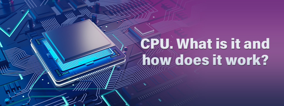
How Does A CPU Work?
In the mid-’60s, the miniaturization revolution began, which led to the idea of packing dozens of semiconductor transistors into a single silicon chip, which spawned an integrated circuit. This laid the foundation for a complete paradigm shift in the development of modern society. In less than a decade, advances in the electronics industry and materials science have led to some of the most amazing progress in human history. In March 1971, a new semiconductor product has commercially launched, which set the stage for this new era.
Every electronic device that you use has some kind of computing module that is a CPU, short for the Central Processing Unit. To understand how the CPU gets its computing power, let's look at what the CPU actually does and how it interacts with digital electronics data.
What does the CPU consist of?

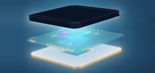 Its
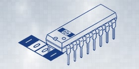
main part is a ceramic substrate whose function is to be strong and not particularly sensitive to temperature. A
microchip made of a huge number of transistors will be fixed on it.
Its
main part is a ceramic substrate whose function is to be strong and not particularly sensitive to temperature. A
microchip made of a huge number of transistors will be fixed on it.
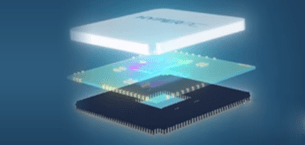 Next
comes the aluminum cover, which has only two functions: to protect this microchip, and to absorb
the heat generated by it.
Next
comes the aluminum cover, which has only two functions: to protect this microchip, and to absorb
the heat generated by it.
The final component is the CPU pins which connect the CPU to the motherboard.
What can a byte tell you?
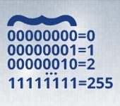 In
the digital world, everything is represented by a binary bit (binary code). This is a rudimentary
representation of two possible states. The view can be represented as zero and one, true or false, up or down, on or
off, etc. The view is physically transmitted to the CPU as a voltage level. If we combine several bits of groups, we
can represent more combinations of discrete states. For example, if we concatenate eight bits together, we get what
is called a byte. It describes 256 different states and can be used to represent numbers. Any
number between 0 and 255 can be specified by a byte. But in the CPU, how we choose to represent the data is
completely changeable. The same byte can, for example, represent a number from minus 128 to plus 127. A byte can
also define other parameters, such as color or sound level.
In
the digital world, everything is represented by a binary bit (binary code). This is a rudimentary
representation of two possible states. The view can be represented as zero and one, true or false, up or down, on or
off, etc. The view is physically transmitted to the CPU as a voltage level. If we combine several bits of groups, we
can represent more combinations of discrete states. For example, if we concatenate eight bits together, we get what
is called a byte. It describes 256 different states and can be used to represent numbers. Any
number between 0 and 255 can be specified by a byte. But in the CPU, how we choose to represent the data is
completely changeable. The same byte can, for example, represent a number from minus 128 to plus 127. A byte can
also define other parameters, such as color or sound level.

 When
we concatenate several bytes together, we create what is called a word. Words are determined by the size of the
capacity. A 32-bit word contains 32 bits, a 64-bit word contains 64 bits, and so on. When a CPU is built with its
own word size, it operates on its own architecture.
When
we concatenate several bytes together, we create what is called a word. Words are determined by the size of the
capacity. A 32-bit word contains 32 bits, a 64-bit word contains 64 bits, and so on. When a CPU is built with its
own word size, it operates on its own architecture.
For example, the original intel 4004 CPU ran on a 4-bit word. This means that data passing through the CPU is transmitted in chunks of 4 bits at a time. Modern CPU is usually 64-bit. A 32-bit word, for example, can represent up to 4.2 billion different states of all forms that data within a CPU can take, the most important of which are instructions.
Instruction Set
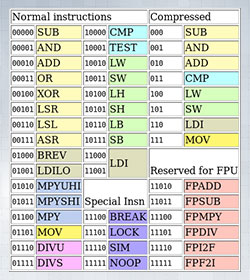 Instructions are unique bits of data that are decoded and executed by the CPU. An example of a
common instruction would be adding two-word meanings together, or moving a data word from one memory location to
another. The entire list of instructions for supported CPU is called the Instruction Set. Each instruction has a
binary representation in the form of machine code, which is usually assigned to a revered representation known as
Assembly Language. If we look at the instruction set of most CPU, they are all centered around performing
mathematical or logical operations, as well as testing data, or moving them from one memory location to another.
Instructions are unique bits of data that are decoded and executed by the CPU. An example of a
common instruction would be adding two-word meanings together, or moving a data word from one memory location to
another. The entire list of instructions for supported CPU is called the Instruction Set. Each instruction has a
binary representation in the form of machine code, which is usually assigned to a revered representation known as
Assembly Language. If we look at the instruction set of most CPU, they are all centered around performing
mathematical or logical operations, as well as testing data, or moving them from one memory location to another.
.jpg)
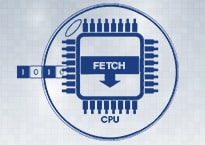
For all purposes and tasks, we can consider the CPU of the machine for processing commands. Their job is to scroll through three main stages: fetching, decoding, and execution. As CPU has evolved, these three stages have become much more complex. Technologies were introduced to expand this basic model of work. In order to fully appreciate these advances, let's first look at the basic mechanics of the CPU.
The main mechanisms of the CPU
 The paradigm of the classic computer reduced instruction set Classic Risc Pipeline, chapters of
the first CPU designs such as the intel 4004. At the extraction stage, the CPU is loaded with an instruction that
will be executed. The central CPU can be imagined as being in an information bubble. It retrieves information data
from the outside, performs an operation in its internal environment, and then returns the data back.
The paradigm of the classic computer reduced instruction set Classic Risc Pipeline, chapters of
the first CPU designs such as the intel 4004. At the extraction stage, the CPU is loaded with an instruction that
will be executed. The central CPU can be imagined as being in an information bubble. It retrieves information data
from the outside, performs an operation in its internal environment, and then returns the data back.
This data is usually stored in external memory of the CPU called Random Access Memory or RAM. Programming instructions data are loaded into RAM from more persistent sources such as hard drives and flash memory.
 The
CPU loads data words by requesting the contents of a particular cell from RAM, this is called a Data Address (or
simply Address). The amount of data that the CPU can address at one time is determined by its address capacity. For
example, a 4-bit address can only directly address 16 data locations. There are mechanisms for addressing more data
than the address capacity of the CPU.
The
CPU loads data words by requesting the contents of a particular cell from RAM, this is called a Data Address (or
simply Address). The amount of data that the CPU can address at one time is determined by its address capacity. For
example, a 4-bit address can only directly address 16 data locations. There are mechanisms for addressing more data
than the address capacity of the CPU.
 The
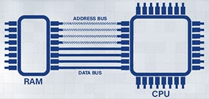
mechanism by which data is moved back and forth to the main memory is called Buses. The bus can be
thought of as a multi-lane trunk between the CPU and RAM, with each bit of data having its own bandwidth. But we
also need to pass the location of the data we are requesting, so we need to add a second trunk that takes into
account both the size of the data word and the word of the address. They are called data bus and
address bus respectively.
The
mechanism by which data is moved back and forth to the main memory is called Buses. The bus can be
thought of as a multi-lane trunk between the CPU and RAM, with each bit of data having its own bandwidth. But we
also need to pass the location of the data we are requesting, so we need to add a second trunk that takes into
account both the size of the data word and the word of the address. They are called data bus and
address bus respectively.
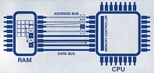 In
practice, these data and address lines, or physical electrical connections between the CPU and RAM, often look like
a super backbone on a printed circuit board. When the CPU makes a request to access RAM, the CPU's memory management
area loads the address bus with the address of the memory word it wants to access. Then it starts a control line
that signals a read request from memory. Upon receipt of this request, the RAM sends the contents of the requested
memory cell over the data bus. Now the CPU can see its data on the bus.
In
practice, these data and address lines, or physical electrical connections between the CPU and RAM, often look like
a super backbone on a printed circuit board. When the CPU makes a request to access RAM, the CPU's memory management
area loads the address bus with the address of the memory word it wants to access. Then it starts a control line
that signals a read request from memory. Upon receipt of this request, the RAM sends the contents of the requested
memory cell over the data bus. Now the CPU can see its data on the bus.

Writing data to RAM works in a similar way, only in this case the CPU sends data to the data bus. When the main memory receives the correct signal, the contents of the data bus are written to the location in the main memory pointed to by the address bus.
.jpg)
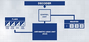
The address of the memory location to be retrieved is stored in an area of the CPU called the Register. A register is a high-speed word in the CPU's internal memory that is used as a scratchpad for CPU operations. It is usually used as a temporary data store for instructions. It can also be assigned to vital CPU functions such as keeping track of the current address being accessed in RAM.

As
soon as a word of memory is read into the CPU, the contents of the register that stores the address of that word are
incremented by one. This register is called the Program Counter. In the next cycle of learning, it receives the next
instruction with a sequence. Access to RAM data is usually the bottleneck for the CPU, due to the need to interact
with components physically remote from the CPU core.
Once the instruction is received, the decoding phase
begins. In classical RISC architecture, one word of memory contains complete instruction. This method has changed to
more complex ones as CPU evolved and moved to CISC.
When the instruction is decoded, the word is split into two parts known as Bit Fields: an opcode and an operand. An opcode is a unique series of bits that represents a specific function in the CPU. Usually, opcodes instructing the CPU to move the data into a register - LDM (Load Data to Accumulator Register), move data between register and memory - WRM (Write Accumulator Register to RAM), perform math and logic functions in a register - ADD (Add to Accumulator Register), and branch out - LCN (Jump on Condition Test). The opcode sometimes needs data to complete its operation. This part of the instruction is called the operand. An operand is a series of bits inserted into instruction to be used as data.

.jpg)
 Once we
have our opcode and operand, the opcode is matched through a table and a combination of charts, where the control
unit then configures the various operating sections of the CPU to perform the operation. In some modern CPUs, the
encoding phase is not hardware-based and can be programmed with microcode. This allows you to change how the
construct is decoded and the CPU is configured for execution. The execution phase of the now configured CPU has
started. This can happen in one step, or in a series of steps, depending on the opcode.
Once we
have our opcode and operand, the opcode is matched through a table and a combination of charts, where the control
unit then configures the various operating sections of the CPU to perform the operation. In some modern CPUs, the
encoding phase is not hardware-based and can be programmed with microcode. This allows you to change how the
construct is decoded and the CPU is configured for execution. The execution phase of the now configured CPU has
started. This can happen in one step, or in a series of steps, depending on the opcode.
One
of the most commonly used CPU sections during execution is the Arithmetic Logic Unit or ALU. This block of circuits
is designed to receive two operands, perform arithmetic or bitwise logical operations on them. The results are then
output along with the appropriate math flags such as carryover and overflow, or a zero result. The result of the ALU
calculation is then sent to either a register or a memory location based on the opcode.
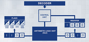 Suppose, for example, the instruction requires adding the number 10 to a register and placing
the result in this register. The CPU control unit will load the direct instruction value into the ALU, load the
register value into the ALU, and then connect the ALU output to the register. On the execution trigger, the
summation will be performed, and the result is loaded into the register. In fact, the software goes through a cycle
of configuring the group circuits to communicate with each other in the CPU.
Suppose, for example, the instruction requires adding the number 10 to a register and placing
the result in this register. The CPU control unit will load the direct instruction value into the ALU, load the
register value into the ALU, and then connect the ALU output to the register. On the execution trigger, the
summation will be performed, and the result is loaded into the register. In fact, the software goes through a cycle
of configuring the group circuits to communicate with each other in the CPU.
.jpg) In the CPU, these 3 phases are continuously cycled. Following the instructions, the computer
program is loaded into memory and synchronized with the clock frequency. It is a repetitive pulse used to
synchronize the internal mechanism of the CPU, its interface with external components. The clock speed of a CPU is
measured in pulses per second or hertz.
In the CPU, these 3 phases are continuously cycled. Following the instructions, the computer
program is loaded into memory and synchronized with the clock frequency. It is a repetitive pulse used to
synchronize the internal mechanism of the CPU, its interface with external components. The clock speed of a CPU is
measured in pulses per second or hertz.
Modern CPUs can maintain clock speeds approaching 5 gigahertz, or 5 billion pulses per second. On simpler CPUs, one cycle starts the fetching, decoding, and execution stage. As a CPU becomes more complex, these steps can take several clock cycles. Optimizing these phases of their use of clock cycles is key to increasing processing power. The bandwidth of the CPU, or the number of instructions that can be executed, determines its speed. By increasing the clock speed, we can make the CPU go through stages faster. However, as we increase the clock speed, we face new challenges. The interval between ticks should allow enough time for each possible command combination to be executed. If a new clock pulse occurs before the instruction cycle completes, the results become unpredictable and the program will fail. In addition, increasing the clock frequency has the side effect of increasing power dissipation and heat build-up in the CPU, resulting in degraded circuit performance.